13691035797
Contact Us
русский
简体中文
English
All Products
Optical Device
Optical Equipment
Optical Fiber
Modulator/photodetector
Radio Frequency Module
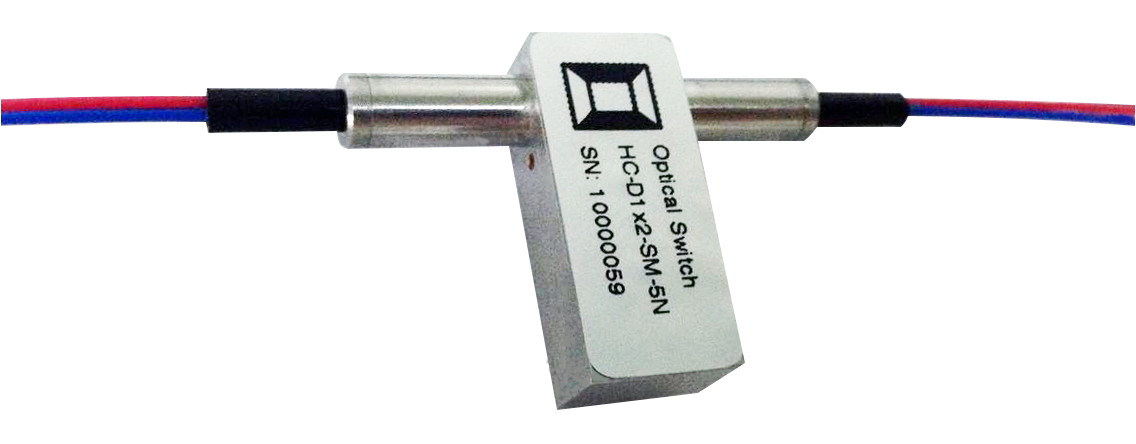
Optical Switch(OSW/FSW/MEMS/OCS)
MEMS Optical Switch
ByPass Optical Switch
Magnet Optical Switch
Miniature optical switch
Mechanical Optical Switch
Optical Switch Matrix Module
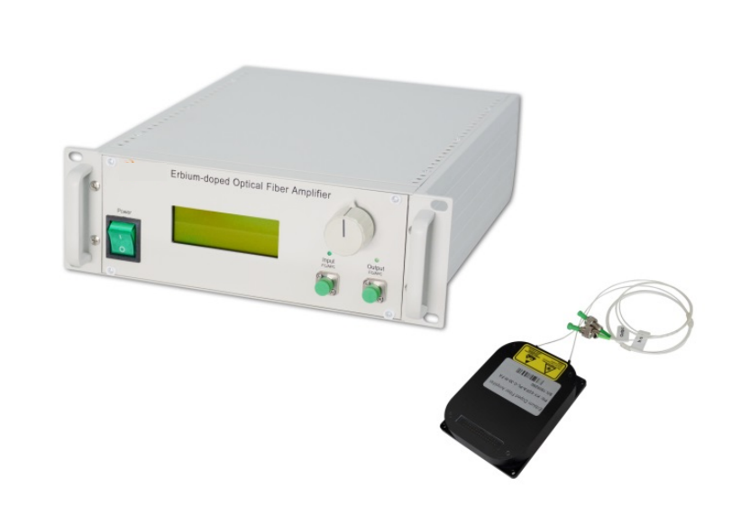
Optical Amplifier
Raman Fiber Amplifer( RFA)
Fiber Optical Amplifier EDFA
High Power Optical Amplifier EDFA
Polarization Maintaining Erbium-doped Fiber Amplifier
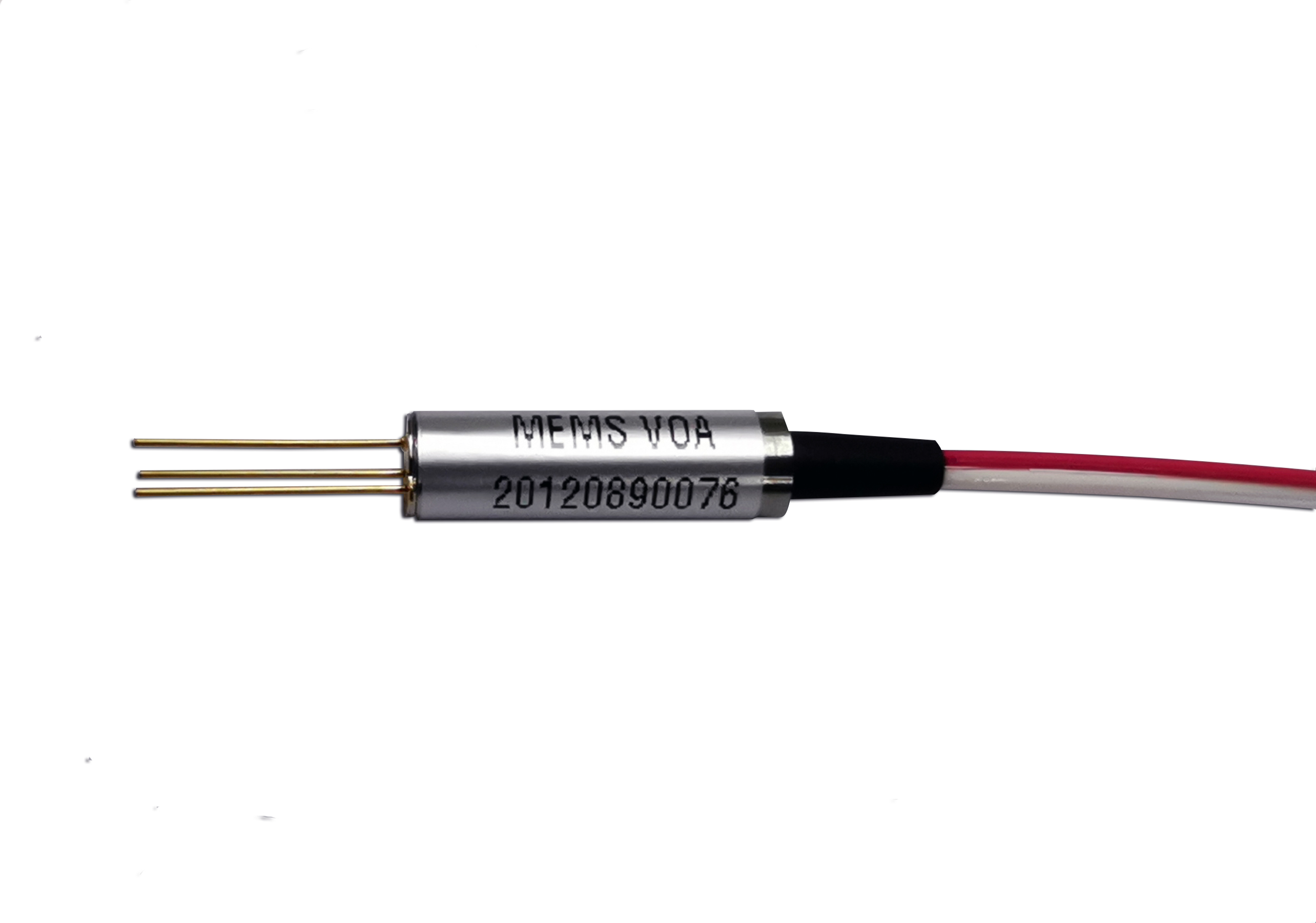
Variable Optical Attenuator
MEMS VOA
Mini MEMS VOA
PM MEMS Attenuator
Other Type Attenuator
Optical Attenuation Module
532-2050 nm PM Attenuator
lsolator
Fiber Isolator
Free-Space Isolator
Polarizing Maintain Device
PM WDM
PM Coupler
PM Attenuator
PM Mini Optical Switch
PM MEMS Optical Switch
PM Other Optical Devices
PM Magneto-Optical Switch
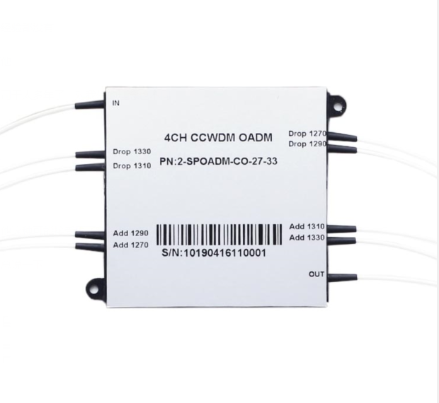
WDM
AWG
CWDM
DWDM
FWDM
CCWDM
LAN WDM
ISO+WDM
Fused WDM
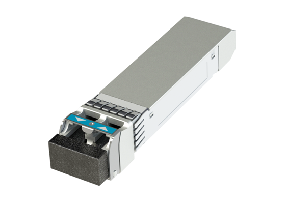
SFP Transceiver Module
1.25G
10G
25G
40G
100G
400G
2.5G/3.125G
Laser and Biomedical Applications
Polarizer
Circulator
PM Splitter/Combiner
High Power Fiber Isolator
Faraday Rotator /Faraday Mirror
High Power Wavelength Division Multiplexer
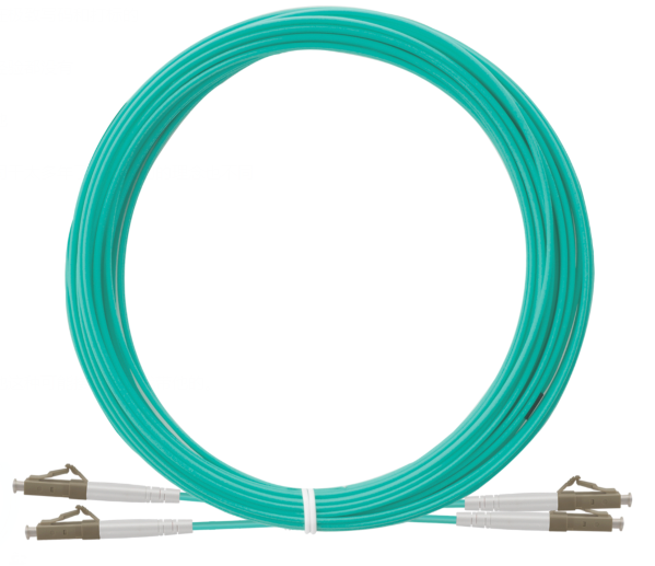
Patch Cord & Flange
Loopback
Patch Cord
MPO Patch Cord
OTDR Module
OTDR Module
OCM,optical channel monitor
OCM, Optical Channel Monitoring
Other Optical Device
Circulator
Photodetector(PD)
Fiber Optic Adapter
Optical Circuit Switch OCS Equipment
8x8 Optical Circuit Switch OSC
48x48 Optical Circuit Switch OSC
16×16 Optical Circuit Switch OSC
32×32 Optical Circuit Switch OSC
MxN MEMS Optical Circuit Switch OCS Equipment
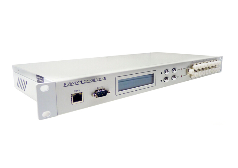
Rack-mounted Optical Switch
1XN Rackmount Optical Switch
1XN Rackmount Multi-mode Optical Switch
2U Rack-Mounted 8-Group 1X6 Optical Switch
DeskTop Optical Switch
Bypass Device
MPO Optical Bypass Switch
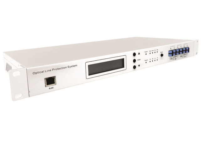
Optical Line Protector(OLP)
Optical Line Protection System
Optical Line protection Module
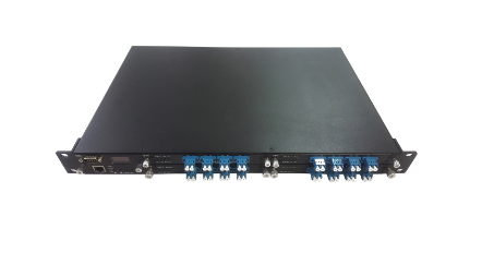
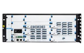
Fiber Cable Monitoring System (OFMS)
Filter Board
WDM Board
OTDR Board
EDFA Fiber Amplifier Board
Optical Source Board (OS Board)
Optical Switch Board (OSW Board)
Optical Power Meter Board (OPM Board)
Fiber Cable Monitoring System(OFMS)
G.652D
G.657A1
G.657A2
Photodetector
PIN photodetector module
Wideband Photoreceiver Module
Balanced optical detection module
APD avalanche photodetection module
Modulator
IQ Modulator
Hot
Phase Modulator
Hot
Intensity Modulator
Hot
Butterfly-shaped SOA
SOA pulse modulation module
Fast Tunable Laser Source Module
High-power low-noise semiconductor laser
SOA pulse modulation and amplification module
Hot
Fiber Bragg grating sensor demodulation module
Radio over Fiber(RFoF)
Solutions
Communication Solution
Line Monitoring Solution
Sensing Solution
DWDM Product Technical Exchange
AI Intelligent Computing Centre
Line Monitoring Solution
Services
Services and Supports
Try professional and convenient services of HC to push your projects into success.
HC Services
Product Services
Solution Services
Demo Support Center
After Sales Service
Help Center
Help Center
Expert Team Support
Free Support for Members 5*24 Online Service
Resources
Resources
Resource Center that assists customers in problem-solving through providing a rich array of product resources.
In the News
Company News
Industry News
Easy access to all product resource information
In the News
Company News
Industry News
About Us
About Us
HC OPTICAL takes optical communication, Internet of Things and data center as the core business development, focusing on the research and development, production and sales of communication devices, integrated equipment and other products, and providing one-stop overall solutions for communication/data and other fields.
Explore HC
Overview
Qualification
Production Line
Contact Us
lina@glhcoptical.com
13691035797
Contact Us
X
Search
Cancel
X
13691035797
русский
简体中文
English
×
Optical Device
›
Optical Switch(OSW/FSW/MEMS/OCS)
›
MEMS Optical Switch
ByPass Optical Switch
Magnet Optical Switch
Miniature optical switch
Mechanical Optical Switch
Optical Switch Matrix Module
Optical Amplifier
›
Raman Fiber Amplifer( RFA)
Fiber Optical Amplifier EDFA
High Power Optical Amplifier EDFA
Polarization Maintaining Erbium-doped Fiber Amplifier
Variable Optical Attenuator
›
MEMS VOA
Mini MEMS VOA
PM MEMS Attenuator
Other Type Attenuator
Optical Attenuation Module
532-2050 nm PM Attenuator
lsolator
›
Fiber Isolator
Free-Space Isolator
Polarizing Maintain Device
›
PM WDM
PM Coupler
PM Attenuator
PM Mini Optical Switch
PM MEMS Optical Switch
PM Other Optical Devices
PM Magneto-Optical Switch
WDM
›
AWG
CWDM
DWDM
FWDM
CCWDM
LAN WDM
ISO+WDM
Fused WDM
SFP Transceiver Module
›
1.25G
10G
25G
40G
100G
400G
2.5G/3.125G
Laser and Biomedical Applications
›
Polarizer
Circulator
PM Splitter/Combiner
High Power Fiber Isolator
Faraday Rotator /Faraday Mirror
High Power Wavelength Division Multiplexer
Patch Cord & Flange
›
Loopback
Patch Cord
MPO Patch Cord
OTDR Module
›
OTDR Module
OCM,optical channel monitor
›
OCM, Optical Channel Monitoring
Other Optical Device
›
Circulator
Photodetector(PD)
Fiber Optic Adapter
Optical Equipment
›
Optical Circuit Switch OCS Equipment
›
8x8 Optical Circuit Switch OSC
48x48 Optical Circuit Switch OSC
16×16 Optical Circuit Switch OSC
32×32 Optical Circuit Switch OSC
MxN MEMS Optical Circuit Switch OCS Equipment
Rack-mounted Optical Switch
›
1XN Rackmount Optical Switch
1XN Rackmount Multi-mode Optical Switch
2U Rack-Mounted 8-Group 1X6 Optical Switch
DeskTop Optical Switch
Bypass Device
›
MPO Optical Bypass Switch
Optical Line Protector(OLP)
›
Optical Line Protection System
Optical Line protection Module
Fiber Cable Monitoring System (OFMS)
›
Filter Board
WDM Board
OTDR Board
EDFA Fiber Amplifier Board
Optical Source Board (OS Board)
Optical Switch Board (OSW Board)
Optical Power Meter Board (OPM Board)
Fiber Cable Monitoring System(OFMS)
Optical Fiber
›
G.652D
G.657A1
G.657A2
Modulator/photodetector
›
Photodetector
›
PIN photodetector module
Wideband Photoreceiver Module
Balanced optical detection module
APD avalanche photodetection module
Modulator
›
IQ Modulator
Phase Modulator
Intensity Modulator
Butterfly-shaped SOA
SOA pulse modulation module
Fast Tunable Laser Source Module
High-power low-noise semiconductor laser
SOA pulse modulation and amplification module
Fiber Bragg grating sensor demodulation module
Radio Frequency Module
›
Radio over Fiber(RFoF)
Solutions
›
Communication Solution
›
DWDM Product Technical Exchange
AI Intelligent Computing Centre
Line Monitoring Solution
›
Line Monitoring Solution
Sensing Solution
›
Services
›
HC Services
›
Product Services
Solution Services
Demo Support Center
After Sales Service
Help Center
›
Help Center
Resources
›
Company News
Industry News
About Us
›
Overview
Qualification
Production Line
Email:
lina@glhcoptical.com
Phone:
13691035797
Optical Device
Optical Equipment
Optical Fiber
Modulator/photodetector
Radio Frequency Module
Optical Switch(OSW/FSW/MEMS/OCS)
MEMS Optical Switch
ByPass Optical Switch
Magnet Optical Switch
Miniature optical switch
Mechanical Optical Switch
Optical Amplifier
Raman Fiber Amplifer( RFA)
Fiber Optical Amplifier EDFA
High Power Optical Amplifier EDFA
Polarization Maintaining Erbium-doped Fiber Amplifier
Variable Optical Attenuator
MEMS VOA
Mini MEMS VOA
PM MEMS Attenuator
Other Type Attenuator
Optical Attenuation Module
lsolator
Fiber Isolator
Free-Space Isolator
Polarizing Maintain Device
PM WDM
PM Coupler
PM Attenuator
PM Mini Optical Switch
PM MEMS Optical Switch
WDM
AWG
CWDM
DWDM
FWDM
CCWDM
SFP Transceiver Module
1.25G
10G
25G
40G
100G
Laser and Biomedical Applications
Polarizer
Circulator
PM Splitter/Combiner
High Power Fiber Isolator
Faraday Rotator /Faraday Mirror
Patch Cord & Flange
Loopback
Patch Cord
MPO Patch Cord
OTDR Module
OTDR Module
OCM,optical channel monitor
OCM, Optical Channel Monitoring
Other Optical Device
Circulator
Photodetector(PD)
Fiber Optic Adapter
Optical Circuit Switch OCS Equipment
8x8 Optical Circuit Switch OSC
48x48 Optical Circuit Switch OSC
16×16 Optical Circuit Switch OSC
32×32 Optical Circuit Switch OSC
MxN MEMS Optical Circuit Switch OCS Equipment
Rack-mounted Optical Switch
1XN Rackmount Optical Switch
1XN Rackmount Multi-mode Optical Switch
2U Rack-Mounted 8-Group 1X6 Optical Switch
DeskTop Optical Switch
Bypass Device
MPO Optical Bypass Switch
Optical Line Protector(OLP)
Optical Line Protection System
Optical Line protection Module
Fiber Cable Monitoring System (OFMS)
Filter Board
WDM Board
OTDR Board
EDFA Fiber Amplifier Board
Optical Source Board (OS Board)
Photodetector
PIN photodetector module
Wideband Photoreceiver Module
Balanced optical detection module
APD avalanche photodetection module
Modulator
IQ Modulator
Phase Modulator
Intensity Modulator
Butterfly-shaped SOA
SOA pulse modulation module
Company News
New product launch
SVIAZ 2026- booth number is 2E086
China-Central Asia (Uzbekistan) Trade Exhibition 2025
Utility model patent----"A matrix optical switching device"
Mechanical optical switches with low loss, polarization-maintaining optical switches
New optical switch: 1000um extra-large optical fiber optical switch
MEMS optical switch Module
New patent certificate
New patent certificate
Custom frame mounted optical switch
More+
Industry News
Feature Solutions
DWDM Product Technical Exchange
AI Intelligent Computing Centre
Line Monitoring Solution
DWDM Product Technical Exchange
AI Intelligent Computing Centre
Line Monitoring Solution
Services
Product Services
Solution Services
Demo Support Center
After Sales Service
Product Services
Solution Services
Demo Support Center
After Sales Service