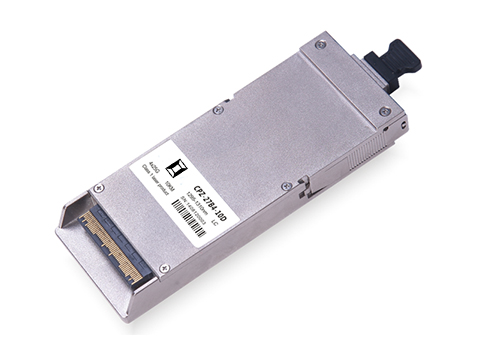
Product Features
Compliant with 100GBASE-LR4
Support line rates from 103.125 Gbps to 111.81 Gbps
Integrated LAN WDM TOSA / ROSA for up to 10 km reach over SMF
Digital Diagnostics Monitoring Interface
Duplex LC optical receptacle
No external reference clock
Single 3.3 V power supply
Case operating temperature range:0°C to 70°C
Power dissipation < 6W
Application
Local Area Network (LAN)
Data Center
Ethernet switches and router applications
Standard
Compliant to IEEE 802.3ba
Compliant to CFP MSA CFP2 Hardware Specification
Compliant to CFP MSA Management Interface Specification
General Description
HC 100G CFP2 LR4 optical Transceiver integrates receiver and transmitter path on one module. In the transmit side, four lanes of serial data streams are recovered, retimed, and passed to four laser drivers. The laser drivers control four EMLs (Electric-absorption Modulated Lasers) with center wavelength of 1296 nm, 1300nm, 1305nm and 1309 nm. The optical signals are multiplexed to a single –mode fiber through an industry standard LC connector. In the receive side, the four lanes of optical data streams are optically de-multiplexed by the integrated optical de-multiplexer. Each data stream is recovered by a PIN photo-detector and transimpedance amplifier, retimed. This module features a hot-pluggable electrical interface, low power consumption and MDIO management interface.
The module provides an aggregated signaling rate from 103.125 Gbps to 111.81 Gbps. It is compliant with IEEE 802.3-2012 Clause 88 100GBASE-LR4 and ITU-T G.959.1-2012-02, and OIF2010.404.08 CEI-28G-VSR electrical specifications. The MDIO management interface complies with IEEE 802.3-2012 Clause 45 standard. The transceiver complies with CFP MSA CFP2 Hardware Specification Rev. 1.0, CFP MSA Management Interface Specification Rev. 2.2, and OIF CEI-28G-VSR standards. A block diagram is shown in Figure 1.

Figure 1. CFP2 LR4 Optical Transceiver functional block diagram
Transmitter
The transmitter path converts four lanes of serial NRZ electrical data from line rate of 25.78 Gbps to 27.95 Gbps to a standard compliant optical signal. Each signal path accepts a 100 Ω differential 100 mV peak-to-peak to 900 mV peak-to-peak 25 Gbps electrical signal on TDxn and TDxp pins. Inside the module, each differential pair of electric signals is input to a CDR (clock-data recovery) chip. The recovered and retimed signals are then passed to a laser driver which transforms the small swing voltage to an output modulation that drives a EML laser. The laser drivers control four EMLs with center wavelengths of 1296 nm, 1300 nm, 1305 nm and 1309 nm. The optical signals from the four lasers are multiplexed together optically. The combined optical signals are coupled to single-mode optical fiber through an industry standard LC optical connector.
Receiver
The receiver takes incoming combined four lanes optical data from line rate of 25.78 Gbps to 27.95 Gbps through an industry standard LC optical connector. The four incoming wavelengths are separated by an optical de-multiplexer into four separated channels. Each output is coupled to a PIN photo-detector. The electrical currents from each PIN photo-detector are converted to a voltage with a high-gain transimpedance amplifier. The electrical output is recovered and retimed by the CDR chip. The four lanes of reshaped electrical signals are output to RDxp and RDxn pins.
Low Speed Signaling
Low speed signaling is based on low voltage CMOS (LVCMOS) operating at a nominal voltage of 3.3 V for the control and alarm signals, and at a nominal voltage of 1.2 V for MDIO address, clock and data signals. All low speed inputs and outputs are based on the CFP MSA CFP2 Hardware Specification Rev. 1.0 and CFP MSA Management Interface Specification Rev. 2.2 requirements.
MDC/MDIO: Management interface clock and data lines.
PRTADR0, 1, 2: Input pins. MDIO physical port addresses.
GLB_ALEMn: Output pin. When asserted low indicates that the module has detected an alarm condition in any MDIO alarm register.
PRG_CNTL1, 2, 3: Input pins. Programmable control lines defined in the CFP MSA Management Interface Specification. Pulled up with 4.7 kΩ to 10 kΩ resistors to 3.3 V inside the CFP2 module.
TX_Disable: Input pin. When asserted high or left open the transmitter output is turned off. When Tx_Dsiable is asserted low or grounded the module transmitter is operating normally. Pulled up with 4.7 kΩ to 10 kΩ resistors to 3.3 V inside the CFP2 module.
MOD_LOPWR: Input pin. When asserted high or left open the CFP2 module is in low power mode. When asserted low or grounded the module is operating normally. Pulled up with 4.7 kΩ to 10 kΩ resistors to 3.3 V inside the CFP2 module.
MOD_RSTn: Input pin. When asserted low or grounded the module is in Reset mode. When asserted high or left open the CFP2 module is operating normally after an initialization process. Pulled down with 4.7 kΩ to 10 kΩ resistors to ground inside the CFP2 module.
PRG_ALRM1, 2, 3: Output pins. Programmable alarm lines defined in the CFP MSA Management Interface Specification.
Mod_ABS: Output pin. Asserted high when the CFP2 module is absent and is pulled low when the CFP2 module is inserted.
RX_LOS: Output pin. Asserted high when insufficient optical power for reliable signal reception is received.
Pin Function Definitions

Figure 2 CFP2 optical transceiver pin-out
Absolute Maximum Ratings
Parameter | Symbol | Min. | Typ. | Max. | Unit | Note |
Storage Temperature | Ts | -40 | - | 85 | ºC | |
Relative Humidity | RH | 5 | - | 95 | % | |
Power Supply Voltage | VCC | -0.3 | - | 4 | V | |
Signal Input Voltage | Vcc-0.3 | - | Vcc+0.3 | V | ||
Receive Input Optical Power (Damage threshold) | Pdmg | 5.0 | dBm |
Low Speed Electrical Characteristics
![(`SYIY%3]Q7_}%I]JI@~{_Y.png](/uploads/20230328/202303281103068625.png "(`SYIY%3]Q7_}%I]JI@~{_Y.png")
High Speed Electrical Specifications
Parameter | Symbol | Min | Max | Unit | Notes |
Transmitter electrical input from host | |||||
Differential voltage pk-pk | 900 | mV | |||
Common mode noise (rms) | 17.5 | mV | |||
Differential termination mismatch | 10 | % | |||
Transition time | 10 | ps | 20/80% | ||
Common mode voltage | -0.3 | 2.8 | V | ||
Eye width | EW15 | 0.46 | UI | At10-15probability | |
Eye height | EH15 | 100 | mV | At 10-15 probability | |
Receiver electrical output to host | |||||
Differential voltage pk-pk | 900 | mV | |||
Common mode noise (rms) | 17.5 | mV | |||
Differential termination mismatch | 10 | % | |||
Transition time | 9.5 | ps | 20/80% | ||
Vertical eye closure | VEC | 6.5 | dB | ||
Eye width | EW15 | 0.57 | UI | At 10-15 probability | |
Eye height | EH15 | 240 | mV | At 10-15 probability | |
MDIO Management Interface
The HC CFP2 Optical Transceiver incorporates MDIO management interface which is used for serial ID, digital diagnostics, and certain control and status report functions. The CFP2 transceiver supports MDIO pages 8000h NVR 1 Based ID registers, 8080h NVR 2 Extended ID registers, 8100h NVR 3 network lane specific registers , and pages A000h CFP module VR 1 registers,A080h MLG VR 1 registers, A200h network lane VR 1 registers,A280h network lane VR 2 registers.
Details of the protocol and interface are explicitly described in CFP MSA Management Interface Specification. Please refer to the specifications for design reference.
Optical Transmitter Characteristics
Parameter | Symbol | Min | Typ. | Max | Unit | Notes |
Signaling rate, each lane | 25.78125 | GBd | ||||
Lane wavelength(range) | 1294.53 | 1295.56 | 1296.5 9 | nm | ||
1299.02 | 1300.05 | 1301.0 9 | nm | |||
1303.54 | 1304.58 | 1305.6 3 | nm | |||
1308.09 | 1309.14 | 1310.1 9 | nm | |||
Rate tolerance | -100 | 100 | ppm | From nominal rate | ||
Side-mode suppression ratio | SMSR | 30 | dB | |||
Total launch power | 10.5 | dBm | ||||
Average launch power, each lane | Pavg | -4.3 | 4.5 | dBm | ||
Extinction Ratio | ER | 4 | 9 | dB | ||
Optical modulation amplitude, each lane (OMA) |
OMA |
-1.3 |
4.5 |
dBm | ||
Difference in launch power between any two lanes (OMA) |
5 |
dB | ||||
Transmitter and Dispersion Penalty, each lane | TDP | 2.2 | dB | |||
OMA minus TDP, each lane | OMA-TD P | -2.3 | dBm | |||
Average launch power of OFF transmitter, each lane |
-30 |
dBm | ||||
Relative Intensity Noise | RIN20O MA | -130 | dB/Hz | |||
Transmitter reflectance | -12 | dB | ||||
Transmitter eye mask {X1, X2, X3, Y1, Y2, Y3} |
{0.25, 0.4, 0.45, 0.25, 0.28, 0.4} | |||||
Optical Receiver Characteristics
Parameter | Symbol | Min | Typ. | Max | Unit | Notes |
Signaling rate, each lane | 25.78125 | GBd | ||||
Rate tolerance |
-100 |
100 |
ppm | From nominal rate | ||
Average receive power, each lane | Pavg | -10.6 | 4.5 | dBm | ||
Receive power, each lane (OMA) | 4.5 | dBm | ||||
Difference in launch power between any two lanes (OMA) |
5.5 |
dB | ||||
Receiver Sensitivity (OMA), each lane |
Rsen |
-8.6 |
dBm |
1 | ||
Stressed Receiver Sensitivity (OMA), each lane |
SRS |
-6.8 |
dBm | |||
Stressed receiver sensitivity test conditions | ||||||
Vertical eye closure penalty, each lane | VECP | 1.8 | dB | |||
Stressed sys J2 jitter, each lane | J2 | 0.3 | UI | 2 | ||
Stressed sys J9 jitter, each lane | J9 | 0.47 | UI | 2 | ||
Receiver reflectance | -26 | dB | ||||
LOS Assert | Plos_on | -30 | dBm | |||
LOS Deassert | Plos_off | -12 | dBm | |||
LOS Hysteresis | 0.5 | 4 | dB | |||
1. Receiver sensitivity (OMA), each lane, is informative. 2. Vertical eye closure penalty, stressed eye J2 Jitter, and stressed eye J9 Jitter are test conditions for measuring stressed receiver sensitivity. They are not characteristics of the receiver. | ||||||
Outline Dimension(mm)
![7PBEWJX8S]U20(R{[4CJ~XO.png](/uploads/20230328/202303281106043340.png "7PBEWJX8S]U20(R{[4CJ~XO.png")

 Русский