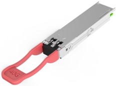
Up to 11.2Gb/s data rate per channel
4 CWDM lanes MUX/DEMUX
Up to 40km transmission
SMF LC duplex connector
QSFP+ MSA compliant
Electrically hot-pluggable
Optical link budget: 16dBm
RoHS-6 compliant and lead-free
Support Digital Monitoring interface
Single +3.3V power supply
Maximum power consumption 3.5W
All-metal housing for superior EMI performance
Case operating temperature Commercial: 0 ~ +70oC Extended: -10 ~ +80oC Industrial: -40 ~ +85oC
40G Ethernet
Data Center
Back to Back
InfiniBand QDR
Absolute Maximum Ratings
It has to be noted that the operation in excess of any individual absolute maximum ratings might cause permanent damage to this module.
Parameter | Symbol | Min | Max | Unit | Notes |
Storage Temperature | TS | -40 | 85 | oC | |
Power Supply Voltage | VCC | 0 | 3.47 | V | |
Relative Humidity (non-condensation) | RH | 5 | 95 | % | |
Damage Threshold | THd | 0 | dBm |
Recommended Operating Conditions
Parameter | Symbol | Min | Typical | Max | Unit | Notes |
Operating Case Temperature |
TOP | 0 | 70 | oC | commercial | |
-40 | 85 | oC | Industrial | |||
Power Supply Voltage | VCC | 3.135 | 3.3 | 3.465 | V | |
Data Rate | 40 | Gb/s | ||||
Control Input Voltage High | 2 | Vcc | V | |||
Control Input Voltage Low | 0 | 0.8 | V | |||
Link Distance (SMF) | D | 40 | km | 9/125um |
Transceiver Block Diagram

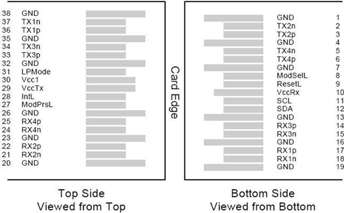
Pin Assignment and Pin Description

Figure1. QSFP+ Transceiver Electrical Pad Layout
PIN | Logic | Symbol | Name/Description | Notes |
1 | GND | Ground | 1 | |
2 | CML-I | Tx2n | Transmitter Inverted Data Input | |
3 | CML-I | Tx2p | Transmitter Non-Inverted Data output | |
4 | GND | Ground | 1 | |
5 | CML-I | Tx4n | Transmitter Inverted Data Input | |
6 | CML-I | Tx4p | Transmitter Non-Inverted Data output | |
7 | GND | Ground | 1 |
8 | LVTLL-I | ModSelL | Module Select | 3 |
9 | LVTLL-I | ResetL | Module Reset | 4 |
10 | VccRx | +3.3V Power Supply Receiver | 2 | |
11 | LVCMOS-I/O | SCL | 2-Wire Serial Interface Clock | 5 |
12 | LVCMOS-I/O | SDA | 2-Wire Serial Interface Data | 5 |
13 | GND | Ground | ||
14 | CML-O | Rx3p | Receiver Non-Inverted Data Output | |
15 | CML-O | Rx3n | Receiver Inverted Data Output | |
16 | GND | Ground | 1 | |
17 | CML-O | Rx1p | Receiver Non-Inverted Data Output | |
18 | CML-O | Rx1n | Receiver Inverted Data Output | |
19 | GND | Ground | 1 | |
20 | GND | Ground | 1 | |
21 | CML-O | Rx2n | Receiver Inverted Data Output | |
22 | CML-O | Rx2p | Receiver Non-Inverted Data Output | |
23 | GND | Ground | 1 | |
24 | CML-O | Rx4n | Receiver Inverted Data Output | 1 |
25 | CML-O | Rx4p | Receiver Non-Inverted Data Output | |
26 | GND | Ground | 1 | |
27 | LVTTL-O | ModPrsL | Module Present | 6 |
28 | LVTTL-O | IntL | Interrupt | 7 |
29 | VccTx | +3.3 V Power Supply transmitter | 2 | |
30 | Vcc1 | +3.3 V Power Supply | 2 | |
31 | LVTTL-I | LPMode | Low Power Mode | 8 |
32 | GND | Ground | 1 | |
33 | CML-I | Tx3p | Transmitter Non-Inverted Data Input | |
34 | CML-I | Tx3n | Transmitter Inverted Data Output | |
35 | GND | Ground | 1 | |
36 | CML-I | Tx1p | Transmitter Non-Inverted Data Input |
37 | CML-I | Tx1n | Transmitter Inverted Data Output | |
38 | GND | Ground | 1 |
Notes:
1. GND is the symbol for signal and supply (power) common for QSFP+ modules. All are common within the QSFP+ module and all module voltages are referenced to this potential unless otherwise noted. Connect these directly to the host board signal common ground plane.
2. VccRx, Vcc1 and VccTx are the receiver and transmitter power suppliers and shall be applied concurrently. Recommended host board power supply filtering is shown in Figure 4 below. Vcc Rx, Vcc1 and Vcc Tx may be internally connected within the QSFP+ transceiver module in any combination. The connector pins are each rated for a maximum current of 500mA.
3. Module Select (ModSelL) is an input pin. When held low by the host, the module responds to 2-wire serial communication commands. The ModSelL allows the use of multiple QSFP+ modules on a single 2-wire interface bus – individual ModSelL lines for each QSFP+ module must be used.
4. The ResetL pin enables a complete module reset, returning module settings to their default state, when a low level on the ResetL pin is held for longer than the minimum pulse length. During the execution of a reset the host shall disregard all status bits until the module indicates a completion of the reset interrupt. The module indicates this by posting an IntL (Interrupt) signal with the Data_Not_Ready bit negated in the memory map. Note that on power up (including hot insertion) the module should post this completion of reset interrupt without requiring a reset.
5. Serial Clock (SCL) and Serial Data (SDA) are required for the 2-wire serial bus communication interface and enable the host to access the QSFP+ memory map.
6. Module Present (ModPrsL) is a signal local to the host board which, in the absence of a module, is normally pulled up to the host Vcc. When a module is inserted into the connector, it completes the path to ground though a resistor on the host board and asserts the signal. ModPrsL then indicates a module is present by setting ModPrsL to a “Low” state.
7. Interrupt (IntL) is an output pin. Low indicates a possible module operational fault or a status critical to the host system. The host identifies the source of the interrupt using the 2-wire serial interface. The IntL pin is an open collector output and must be pulled to the Host Vcc voltage on the Host board
8. Low Power Mode (LPMode) pin is used to set the maximum power consumption for the module in order to protect hosts that are not capable of cooling higher power modules, should such modules be accidentally inserted.

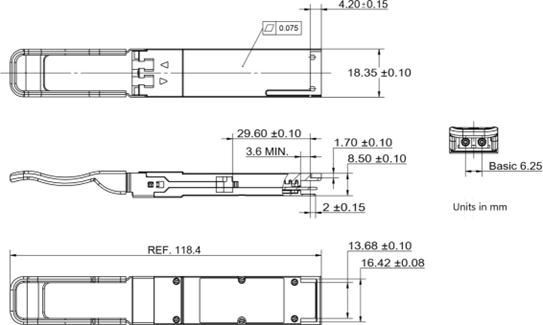
Figure2. Mechanical Outline
Ordering Information
Part Number | Data Rate (Gb/s) | Wavelength (nm) | Transmission Distance(km) | Temperature (oC) (Operating Case) |
HC -QLC41C | 40 |
1271/1291/ 1311/1331 | 40 | 0~70 commercial |
HC -QLC41E | 40 | 40 | -10~80 Extended | |
HC -QLC41I | 40 | 40 | -40~85 Industrial |
If you need more information , Please contact us .