E-mail lina@glhcoptical.com
Up to 11.3Gb/s data rate per channel
Supports 44.6Gb/s aggregate bit rate
Transmitter: cooled 4x10Gb/s LAN WDM EML TOSA (1295.56, 1300.05, 1304.58, 1309.14nm)
Receiver: 4x10Gb/s PIN receiver with SOA
Up to 80km reach for G.652 SMF
Duplex LC optical receptacle
4x10G electrical interface (OIF CEI-28G-VSR)
RoHS-10 compliant and lead-free
Single +3.3V power supply
Maximum power consumption 4.5W
Case operating temperature Commercial: 0 ~ +70 oC, Extended: -10 ~ +80 Oc , Industrial:-40 ~ +85 oC
Applications
40G Ethernet
Data Center
InfiniBand QDR
Absolute Maximum Ratings
It has to be noted that the operation in excess of any individual absolute maximum ratings might cause permanent damage to this module.
Parameter | Symbol | Min | Max | Unit | Notes |
Storage Temperature | TS | -40 | 85 | oC | |
Power Supply Voltage | VCC | -0.3 | 4.0 | V | |
Relative Humidity (non-condensation) | RH | 0 | 85 | % | |
Damage Threshold | THd | -3.0 | dBm |
Recommended Operating Conditions
Parameter | Symbol | Min | Typical | Max | Unit | Notes |
Operating Case Temperature |
TOP | 0 | 70 | oC | commercial | |
-40 | 85 | oC | Industrial | |||
Power Supply Voltage | VCC | 3.135 | 3.3 | 3.465 | V | |
Data Rate, each Lane | 10.3125 | Gb/s | ||||
Control Input Voltage High | 2 | Vcc | V | |||
Control Input Voltage Low | 0 | 0.8 | V | |||
Link Distance (SMF) | D | 80 | km | 1 |
Notes:
1. Depending on actual fiber loss/km (link distance specified is for fiber insertion loss of 0.35dB/km)
Pin Assignment and Pin Description

Figure1. QSFP+ Transceiver Electrical Pad Layout
Pin | Symbol | Name/Description | Notes |
1 | GND | Transmitter Ground (Common with Receiver Ground) | 1 |
2 | Tx2n | Transmitter Inverted Data Input | |
3 | Tx2p | Transmitter Non-Inverted Data output | |
4 | GND | Transmitter Ground (Common with Receiver Ground) | 1 |
5 | Tx4n | Transmitter Inverted Data Input | |
6 | Tx4p | Transmitter Non-Inverted Data output | |
7 | GND | Transmitter Ground (Common with Receiver Ground) | 1 |
8 | ModSelL | Module Select | |
9 | ResetL | Module Reset | |
10 | VccRx | 3.3V Power Supply Receiver | 2 |
11 | SCL | 2-Wire serial Interface Clock | |
12 | SDA | 2-Wire serial Interface Data | |
13 | GND | Transmitter Ground (Common with Receiver Ground) | |
14 | Rx3p | Receiver Non-Inverted Data Output | |
15 | Rx3n | Receiver Inverted Data Output | |
16 | GND | Transmitter Ground (Common with Receiver Ground) | 1 |
17 | Rx1p | Receiver Non-Inverted Data Output | |
18 | Rx1n | Receiver Inverted Data Output | |
19 | GND | Transmitter Ground (Common with Receiver Ground) | 1 |
20 | GND | Transmitter Ground (Common with Receiver Ground) | 1 |
21 | Rx2n | Receiver Inverted Data Output | |
22 | Rx2p | Receiver Non-Inverted Data Output | |
23 | GND | Transmitter Ground (Common with Receiver Ground) | 1 |
24 | Rx4n | Receiver Inverted Data Output | 1 |
25 | Rx4p | Receiver Non-Inverted Data Output | |
26 | GND | Transmitter Ground (Common with Receiver Ground) | 1 |
27 | ModPrsl | Module Present | |
28 | IntL | Interrupt | |
29 | VccTx | 3.3V power supply transmitter | 2 |
30 | Vcc1 | 3.3V power supply | 2 |
31 | LPMode | Low Power Mode | |
32 | GND | Transmitter Ground (Common with Receiver Ground) | 1 |
33 | Tx3p | Transmitter Non-Inverted Data Input | |
34 | Tx3n | Transmitter Inverted Data Output | |
35 | GND | Transmitter Ground (Common with Receiver Ground) | 1 |
36 | Tx1p | Transmitter Non-Inverted Data Input | |
37 | Tx1n | Transmitter Inverted Data Output | |
38 | GND | Transmitter Ground (Common with Receiver Ground) | 1 |
1 GND is the symbol for signal and supply (power) common for QSFP28 modules. All are common within the QSFP28 module and all module voltages are referenced to this potential unless otherwise noted. Connect these directly to the host board signal common ground plane.
1. VccRx, Vcc1 and VccTx are the receiving and transmission power suppliers and shall be applied concurrently. Recommended host board power supply filtering is shown below. Vcc Rx, Vcc1 and Vcc Tx may be internally connected within the QSFP28 transceiver module in any combination. The connector pins are each rated for a maximum current of 1000mA.
The following optical characteristics are defined over the Recommended Operating Environment unless otherwise specified.
Parameter | Symbol | Min. | Typical | Max | Unit | Notes |
Transmitter | ||||||
Lane wavelength(range) | L0 | 1294.53 | 1295.56 | 1296.59 | nm | |
L1 | 1299.02 | 1300.05 | 1301.09 | nm | ||
L2 | 1303.54 | 1304.58 | 1305.63 | nm | ||
L3 | 1308.09 | 1309.14 | 1310.09 | nm | ||
Signaling rate, each lane | 10.3125 | Gb/s | ||||
Side-mode suppression ratio | SMSR | 30 | ||||
Total launch power | Pt | 12 | dBm | |||
Average launch power, each lane |
Pavg |
1 |
6 |
dBm |
1 | |
OMA, each Lane | POMA | 1 | 6 | dBm | 2 | |
Extinction Ratio | ER | 8.2 | dB | |||
Difference in Launch Power between any Two Lanes (OMA) |
Ptx,diff |
3.6 |
dB | |||
Transmitter and Dispersion Penalty, each lane |
TDP |
3.2 |
dB | |||
OMA minus TDP, each lane | OMA-TD P |
-0.65 |
dBm | |||
Average launch power of OFF transmitter, each lane |
Poff |
-30 |
dBm | |||
Transmitter reflectance | RT | -12 | dB | |||
RIN20OMA |
RIN |
-130 | dB/ Hz | |||
Optical Return Loss Tolerance |
TOL |
20 |
dB | |||
Transmitter eye mask {X1, X2,X3, Y1, Y2, Y3} | {0.25, 0.4, 0.45, 0.25, 0.28, 0.4} | |||||
Receiver | ||||||
Signaling rate, each lane | 10.3125 | GBd | ||||
Average Receive Power, each Lane |
-23 |
- 4.9 |
dBm | |||
Receiver Sensitivity, each Lane |
-25 |
dBm |
3 | |||
Input Saturation Power (overload) |
Psat |
-8 |
dBm | |||
Receiver reflectance | -26 | dB | ||||
Difference in Receive Power between any Two Lanes (Average and OMA) |
Ptx,diff |
3.6 |
dB | |||
LOS Assert | LOSA | -35 | dBm | |||
LOS Deassert | LOSD | -26 | dBm | |||
LOS Hysteresis | LOSH | 0.5 | dB | |||
Receiver Electrical 3 dB upper |
Fc |
31 |
GHz | |||
Notes:
2. The minimum average launch power spec is based on ER not exceeding 9.5dB and transmitter OMA higher than 0.1dBm.
3. Even if the TDP < 0.75 dB, the OMA min must exceed the minimum value specified here.
4. Measured with a PRBS=2³¹-1 test pattern @40Gbps, ER=8.2dB, BER≤1E-12.
The following digital diagnostic characteristics are defined over the Recommended Operating Environment unless otherwise specified.
Parameter | Symbol | Min. | Max | Unit | Notes |
Temperature monitor absolute error | DMI_ Temp | -3 | 3 |
oC | Over operating temp |
Supply voltage monitor absolute error | DMI _VCC | -3 | 3 | % | Full operating range |
RX power monitor absolute error | DMI_RX | -3 | 3 | dB | |
Bias current monitor error | DMI_ bias | -10 | 10 | % | |
TX power monitor absolute error | DMI_TX | -3 | 3 | dB | |

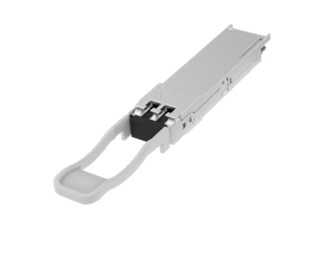
Figure2. Mechanical Outline
Ordering Information
Part Number | Data Rate (Gb/s) | Wavelength (nm) | Transmission Distance(km) | Temperature (oC) (Operating Case) |
HC -QL381C |
40 | 1295.56, 1300.05, 1304.58, 1309.14 |
80km SMF |
0~70 commercial |
HC -QL381E |
40 | 1295.56, 1300.05, 1304.58, 1309.14 |
80km SMF |
-10~80 Extended |
HC -QL381I |
40 | 1295.56, 1300.05, 1304.58, 1309.14 |
80km SMF |
-40~85 Industrial |
If you need more information , Please contact us .

 Русский